Functional Layers for Electronic Applications

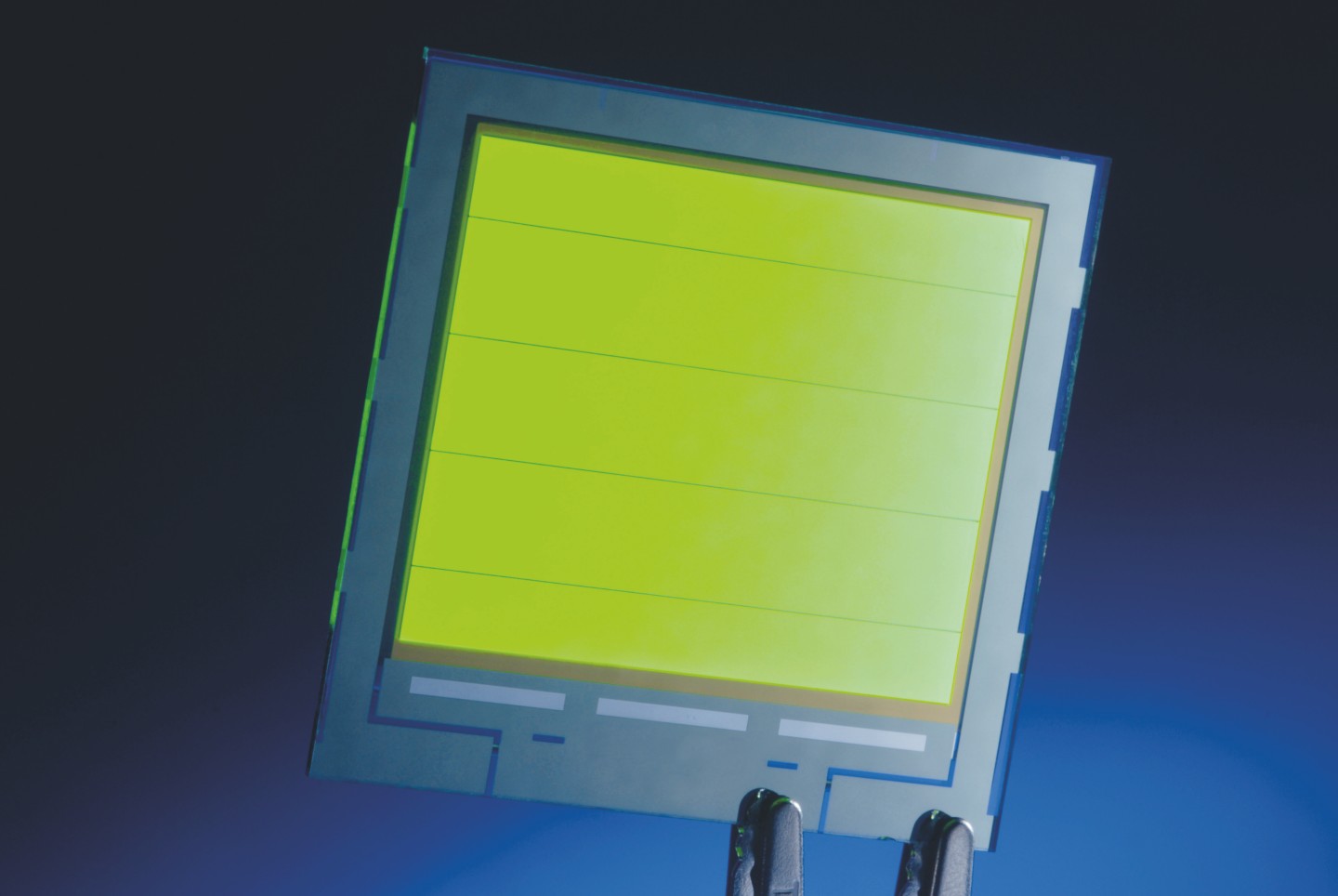
Functional Layers For Electronic Applications

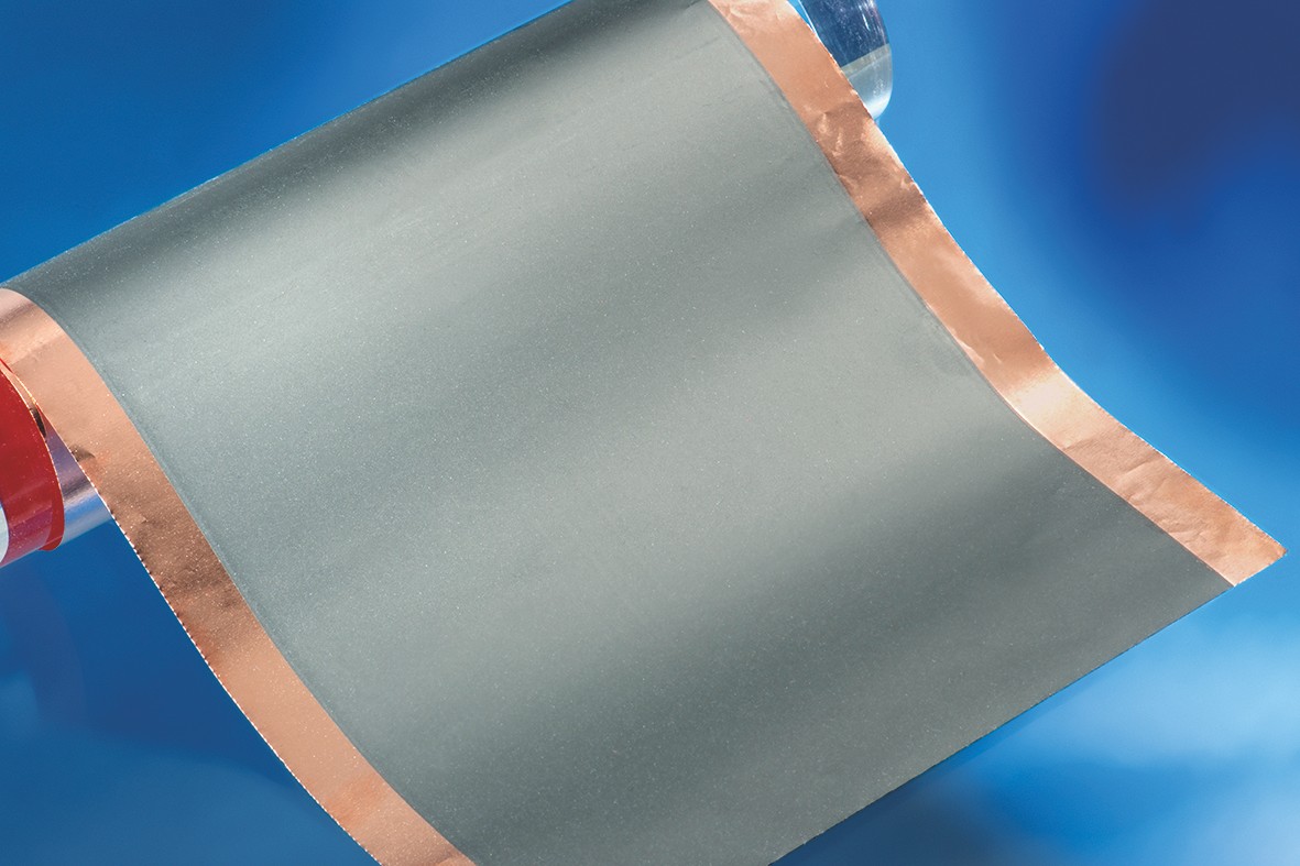
Electronic films are a powerful tool for improving performance of electronic components, adding
functionality and increasing their domain in many areas of modern life.

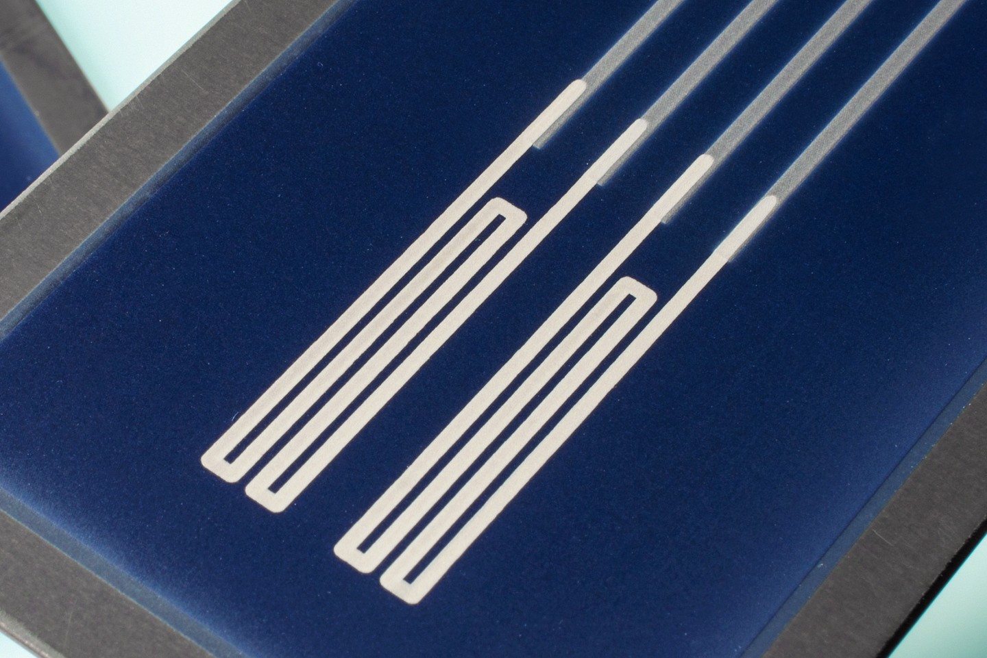
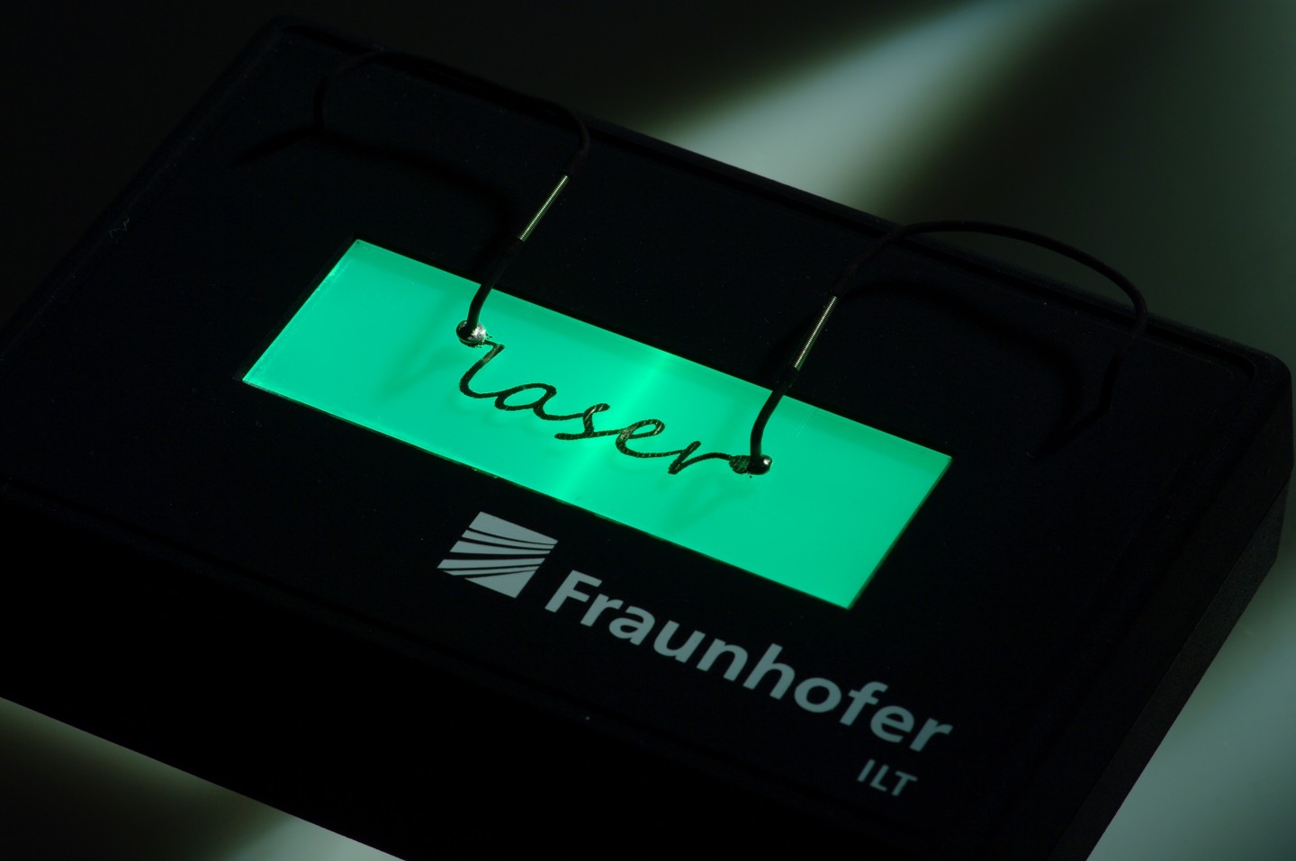
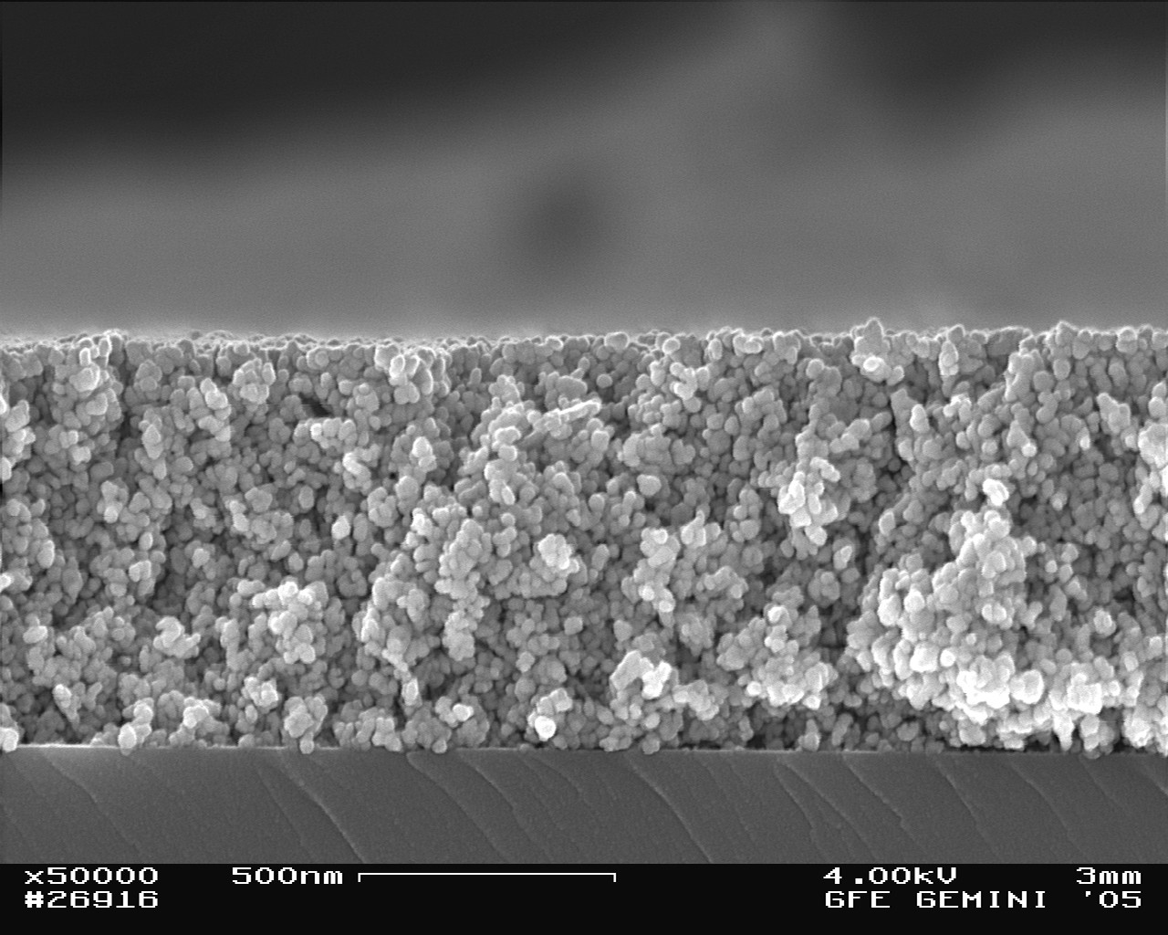
Fraunhofer ILT develops customized solutions for various applications of such films, utilizing either laser treatments of previously applied thin films or combining printing and laser treatment processes to produce electronic layers.

Due to the digital nature of these technologies, they can be used to process batch sizes from millions (mass production) down to only one (individualized production).

LMC – Laser-based Modification of Coatings

Although many electronic components are coated to provide a certain functionality, the coatings often suffer from poor performance or show room for improvement. Laser radiation – thanks to its spectral, temporal and spatial selectivity – can be used to enhance the performance of such coatings by modifying their properties (e.g. by laser (re-)crystallization) within such a short time period that the thermal load on the temperature-sensitive substrate is minimized.

High-Speed Laser Annealing of TCO Coatings

Transparent conductive oxides (TCO) can be found as transparent electrodes in TFTs, OLEDs, touch screens, etc. These 100 nm thick films are usually applied onto display glass via physical or chemical vapor deposition. In contrast to furnaces, laser offers the advantages of selective and locally limited thermal treatment (annealing): In addition to heating and cooling small volumes very quickly, laser radiation generates high film temperatures without damaging the temperature-sensitive substrate. A downstream laser-based annealing process can, thus, be used to further reduce the electrical sheet resistance of indium tin oxide films, for example, by up to 25 %. The visual transparency remains nearly unchanged.

DAPF – Digital Additive Production of Films

Sol-gels as well as nano- and micro-particulate dispersions have proven to be powerful sources for producing functional layers on a wide range of components. Additive techniques such as printing processes show great potential because they permit resource-efficient, flexible and low-cost deposition of structures onto selected areas of the substrate. This represents a considerable challenge, however, as the thermal treatment of these films, crucial to achieve functional properties, often requires temperatures that exceed the temperature stability of the substrate (especially on polymer or glass). The laser beam can overcome these drawbacks due to its high heating
and cooling rates. Thus, post-processing with laser radiation is a key process step for generating layers with appropriate functionality (such as high conductivity, transparency, etc.). The processing steps are typically split up into three phases: laser-based drying, laser-based de-bindering and laser-based functionalization (such as sintering, melting, activation,(re-)crystallization, etc.).

Laser Functionalization of Conductive Films

Conductive paths and pads collect and distribute charge carriers on poorly or non-conducting surfaces. Printed conductive paths on glass or polymers boast a great deal of potential in electronic applications. Printing techniques enable structures to be manufactured from nano- or micro-particulate metallic inks (e.g. copper, silver). Compared with conventional techniques, such as mask or lithographic processes, this process is flexible, inline-capable and saves resources, time and money. The necessary thermal post-treatment for drying, sintering and partially melting the particulate layer is accomplished with laser processes so that temperature-sensitive substrates can continue to be used. Conducting paths can be applied on polymers, glass/ceramics or metals and on prior insulated metals.

Laser Crystallization of Piezoelectric Thin Films

Piezoelectric materials like PZT are used in various electronic devices, such as sensors and actuators. Compared with other methods, the wet chemical sol-gel deposition method has several advantages, such as precise stoichiometry control, low cost and large surface coverage. To crystallize PZT films, a downstream thermal process between 600 and 800 °C is needed.

Unfortunately, conventional rapid thermal annealing (RTA) processes can only be used for thermally stable substrates since these processes heat up not only the PZT film but also the entire substrate. When infrared laser radiation is used, however, the deposited PZT film can be dried, pyrolyzed, and crystallized in an atmospheric environment: 150 nm and thicker PZT films with (111)-preferred texture are generated.

The field-induced strain property is comparable to that of the PZT film fabricated by rapid thermal annealing. The laser crystallization method is expected to open up a new field of PZT applications.

Printed Sensors for Structural Health Monitoring

Printed and laser-functionalized sensor systems for the conjoined monitoring of metallic components can be used to prevent larger damages to massive structural components. After the laser-based surface treatment to increase the films’ mechanical and chemical adhesion, 10 - 30 μm thick printedlayers are dried, de-bindered and sintered or molten via laser  radiation.

Once the steel surface has been initially oxidized and roughened – using laser processes and achieving wettingpromoting and improved adhesive properties – sequences of insulating, conducting and piezo-electric layers can be additively built up to obtain temperature, strain or impact-sound sensors for the monitoring of structural components such as wind turbine bearings, turbine blades, etc.

Laser Drying of Battery Electrodes

In the production of battery electrodes, conventional furnace processes can be substituted by innovative laser processes, providing significant energy savings as well as a considerable reduction of the installation space for the corresponding roll-to-roll system. The laser-based drying process of water-based battery electrode films fulfills the requirement of not exceeding temperatures of 300 °C in the temperature-sensitive, 50 - 100 μm thick films. Laser drying leads to capacities of about 355 mAh/g (similar to conventionally produced cells). Processing rates of about 60 cm²/s can be achieved while the energy consumption is reduced by about 50 %.

This laser-based process can be used in additive manufacturing of dry conventional battery electrodes in mobile devices as well as solid-state electrodes in thin film batteries for small mobile applications (e.g. smart devices, lighted labelling, etc.).