Printed Electronics

printed electronics
© Fraunhofer ILT, Aachen
Brochure Printed Electronics

Printed electronics are opening up more and more fields of application in our everyday lives, for example in OLED displays, solar cells or e-book readers. But which manufacturing processes and materials will determine the applications of the future? The Fraunhofer Institute for Laser Technology ILT develops digital, energy-efficient and resource-saving solutions for such future challenges. 

Printed gold: expensive raw materials used wisely

Today, gold plating for high-quality contact points is produced using electroplating or chemical and physical deposition processes with PVD and CVD. These processes are cost and time intensive and sometimes use environmentally harmful and toxic chemicals. By combining printing and laser processes, the industry can reduce its consumption of cost-intensive precious metals and stop using environmentally harmful chemicals in electroplating processes altogether. Thanks to newly developed laser processes, selectively printed gold pastes can be produced on Ni-Cu substrates. Up to 80 percent of the gold previously used can be saved in this way. The gold layers metallurgically bonded to the substrate material have layer thicknesses of 2 to 5 μm and are mechanically very robust.

Electrical conductors on and in fiber composite plastics

Fiber-reinforced plastics (FRP) have become indispensable in lightweight construction. New manufacturing processes are required, however, as the demand for FRP grows and mechanically monitored, complex structural components or heated components are being functionally integrated into electric aircraft. When digital printing and laser processes are combined, electrical functions (heating, measuring strain, measuring aging, signal lines, etc.) can be integrated on and in FRP. Compared with oven post-treatment processes, this combination process produces layers that put lower thermal stress on the component and that have variable electrical properties.

Piezoelectric actuator coatings

Microelectromechanical systems (MEMS) are turning our smartphones into helpful everyday tools full of useful and compactly integrated functions. Microactuators, such as those in microspeakers or micropumps, are driven by thin piezoelectric functional ceramics that mechanically deform when an electric field is applied. When conventional manufacturing processes are used for microelectronics, producing such piezoelectric multilayer systems is extremely time-consuming and costly. The time and cost required to manufacture highly functional thin-film MEMS on an industrial scale can be reduced significantly, however, by combining inkjet printing with laser-based functionalization processes.

Printing sensors directly onto components

Today, foil strain gages are usually applied to components by hand, a process that requires many steps, experience, time and intuition. Thus, the installation of the strain gauge is usually the largest cost component for using these sensors. Additive manufacturing not only makes it possible to print strain gauges on inexpensive carrier films, strain gauges can also be printed directly onto a component, eliminating the manual step of gluing them on. Coating processes such as dispensing or inkjet printing can apply the necessary functional layers from a digital model in an automated and precise manner. A laser performs the necessary post-treatment in a few seconds without the need to heat the component in an oven. By using a WLAN-capable evaluation board, users can monitor the components wirelessly. In addition to strain gages, temperature sensors, conductive tracks or heating structures can also be applied to the components.

Fraunhofer Institute for Laser Technology ILT

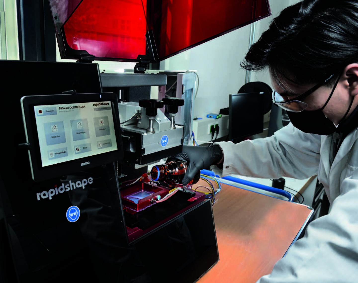
The Fraunhofer Institute for Laser Technology ILT is one of the most important development and contract research institutes in laser development and application worldwide. Its activities encompass a wide range of areas such as developing new laser beam sources and components, laser-based metrology, testing technology and industrial laser processes. This includes laser cutting, ablation, drilling, welding and soldering as well as surface treatment, micro processing and additive manufacturing. Furthermore, Fraunhofer ILT develops photonic components and beam sources for quantum technology. Overall, Fraunhofer ILT is active in the fields of laser plant technology, digitalization, process monitoring and control, simulation and modeling, AI in laser technology and in the entire system technology. We offer feasibility studies, process qualification and laser integration in customized manufacturing lines. The institute focuses on research and development for industrial and societal challenges in the areas of health, safety, communication, production, mobility, energy and environment. Fraunhofer ILT is integrated into the Fraunhofer Gesellschaft.