EUV Lithography

Our range of services

Miniaturization in the electronics and semiconductor industries, among others, increasingly requires metrological and lithographic processes that can detect and modify fine structures in the nanometer and subnanometer range. Here, radiation with very short wavelengths in the EUV (extreme ultraviolet) range – for example, 13.5 nm – is used to manufacture highly precise and complex structural arrangements.

For this purpose, Fraunhofer ILT is developing EUV radiation sources and corresponding methods for material processing and analysis. The EUV technologies are highly sensitive to structures with nanoscale dimensions and can be used advantageously in semiconductor manufacturing. This requires novel photoresists that must simultaneously demonstrate both high sensitivity and high resolution. The EUV exposure system developed at ILT can support the development of such materials in a cost-efficient way.

The range of services we offer includes feasibility studies for customized tasks, the development and realization of customized exposure tools, investigations on the behavior of photoresists and other materials under EUV irradiation, the integration of EUV lithography into manufacturing processes, and individual consulting.

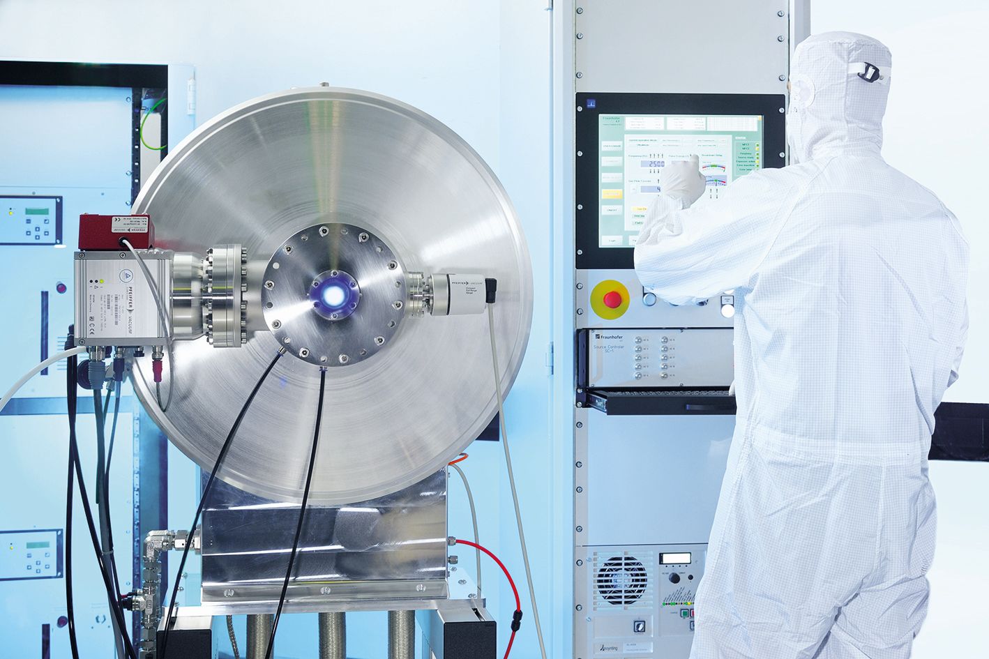
Discharge-based EUV radiation source for wavelengths in the range 2 - 20 nm.
© Fraunhofer ILT, Aachen, Germany.
Discharge-based EUV radiation source for wavelengths in the range 2 - 20 nm.
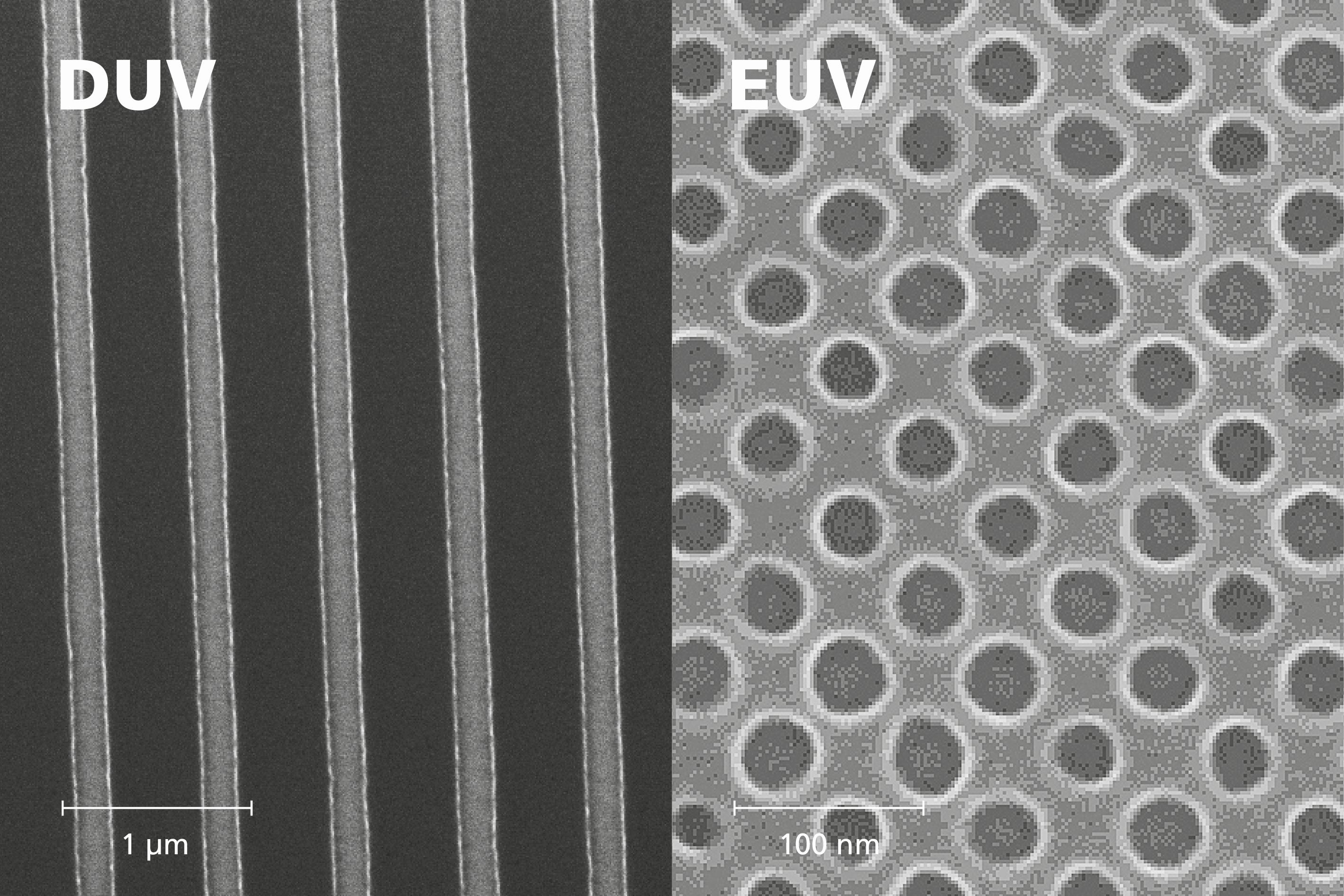
Nanostructures with 300 nm (left, DUV) and 28 nm (right, EUV) half-pitch (HP) generated with laboratory-based EUV source.
© Fraunhofer ILT, Aachen, Germany.
Nanostructures with 300 nm (left, DUV) and 28 nm (right, EUV) half-pitch (HP) generated with laboratory-based EUV source.
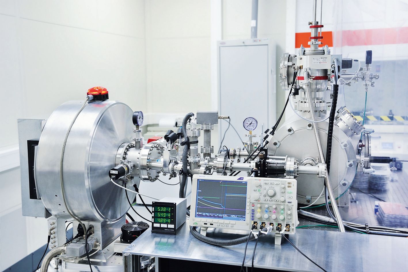
Laboratory system for EUV processing of wafers up to 100 mm diameter.
© Fraunhofer ILT, Aachen, Germany.
Laboratory system for EUV processing of wafers up to 100 mm diameter.

Plasma-based EUV beam sources

  • Beam sources for EUV lithography
  • Beam sources for X-ray microscopy
  • Power electronics
  • Generators for high pulsed currents, fast data acquisition and control of pulsed radiation sources

Plasma generation and diagnostics

  • Gas discharge and laser induced plasmas
  • Spectroscopy from the soft X-ray to the IR range
  • Determination of radiation fluxes
  • Determination of plasma parameters
  • High-speed photography
  • Plasma modeling

System solutions

  • Design of optical systems for EUV applications
  • Optics simulation
  • Integration of plasma radiation sources
  • Realization of complete systems

Applications with EUV radiation

  • X-ray microscopy
  • EUV microscopy for mask inspection
  • EUV reflectometry, analysis of surfaces and layer systems
  • Nanostructuring with EUV interference lithography
  • Characterization of photoresists

Markets

Laser technology can solve demanding tasks in many different industries. Whether as a tool in automotive production, as measuring equipment in the environmental sector, as a diagnostic or therapeutic instrument in medical technology or as a communication medium in space technology, the laser provides multiple uses with high productivity and high efficiency.

Read up about the innovations of the Fraunhofer ILT in a few selected industries and convince yourself!


Research with us!

Please do not hesitate to contact us if you have any questions about general topics! Our contact persons are happy to get in touch with you.

Our services cover a wide range of topics. Related topics and further research and development projects can be found under the following links.