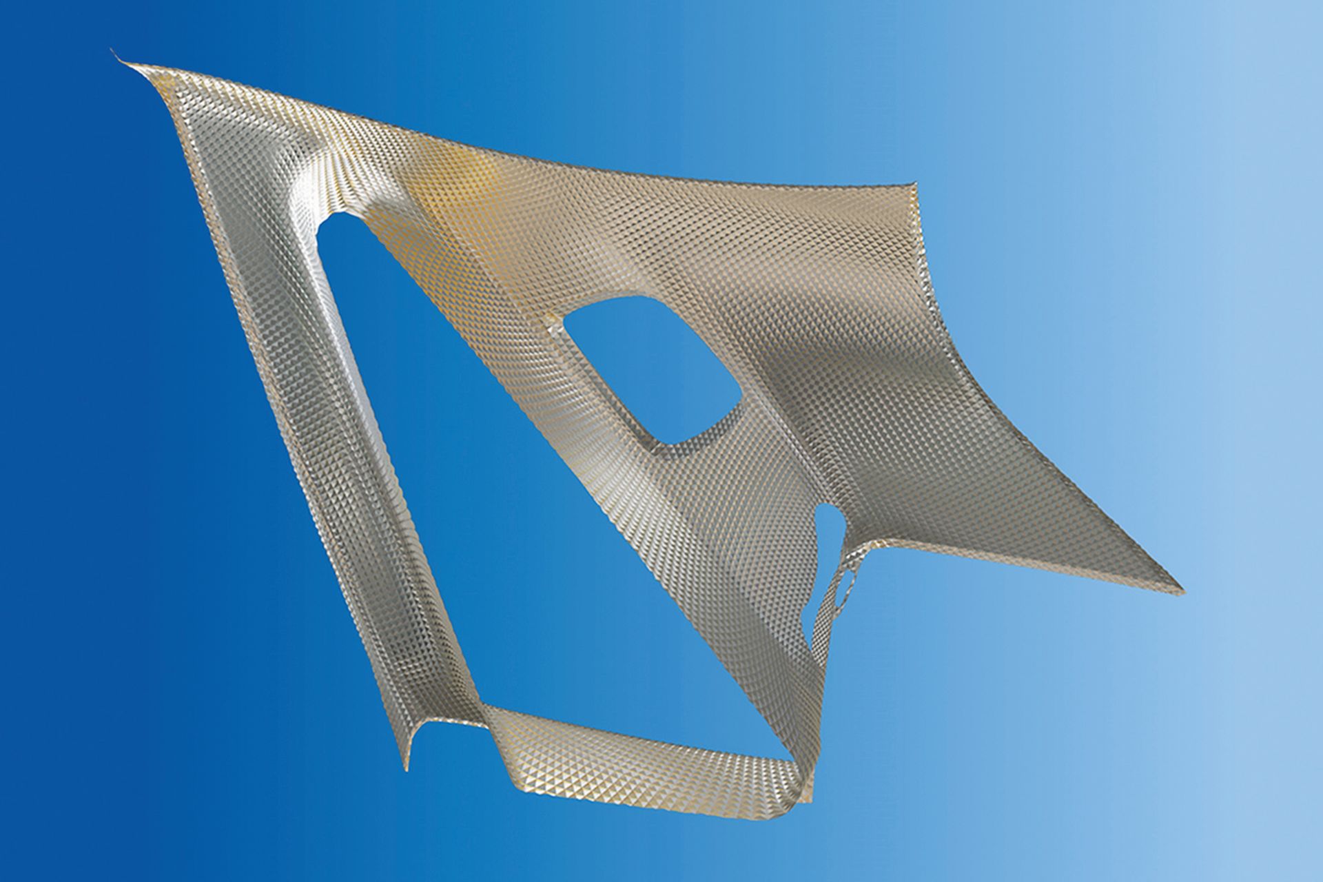
Car makers strive to design vehicle interiors in a way that conveys an impression of superior quality. The finer the texture of the plastic surfaces, the closer they come to approximating the appearance of leather or other high-quality materials. It takes auto suppliers a matter of minutes to fabricate this kind of surface. Manufacturing the instrument panel via injection molding, for example, takes only 60 seconds.
Producing the metal tools required for this purpose takes significantly longer, usually up to four weeks for the tool structuring itself. The three-dimensional texturing is either etched onto the tool in dozens of individual steps or created by means of a laser process with ablation rates in the region of approximately 1 mm³/min.
The eVerest research project saw five companies and three research institutions join forces to radically improve laser structuring technology with resolutions in the micrometer regime.
“Our aim was to make the processes much faster while simultaneously achieving even higher texturing quality,” says Andreas Brenner from the Fraunhofer Institute for Laser Technology ILT, summing up the project’s objectives.
Less scanner dead time and enhanced USP laser power
To optimize the processes, the engineers started out by examining the efficiency of all the components. Significant progress was made by reducing dead times in the scan paths. To achieve this, the team tested new algorithms and worked with scientists at Münster University of Applied Sciences, who evaluated a range of concepts for highly dynamic focusing using convex piezo mirrors. They eventually succeeded in tripling the throughput using innovative scanner technology developed by Scanlab.
The researchers also took the laser technology itself to a new level. Ultrashort pulse (USP) lasers are known for their precision in the nanometer regime. The eVerest team therefore decided to incorporate a USP source in addition to the standard nanosecond (ns) laser. USP lasers have traditionally been criticized for their low productivity. In this case, however, the Fraunhofer ILT process engineers employed a particularly powerful, actively cooled fiber-coupled USP laser from Amphos GmbH – a Fraunhofer ILT’s spin-off and part of the TRUMPF Group since 2018 – to obtain the same ablation rate per watt as that offered by the ns laser. The USP laser makes it possible to reduce surface roughness to less than 0.5 µm.
Quality assurance is also key both during and after processing, and the team evaluated two fiber-coupled OCT systems from Precitec Optronik for this purpose. The inline system facilitates resolutions of 5 µm, while the post-process achieves as low as 1 µm.
Photonic process chain reduces rework
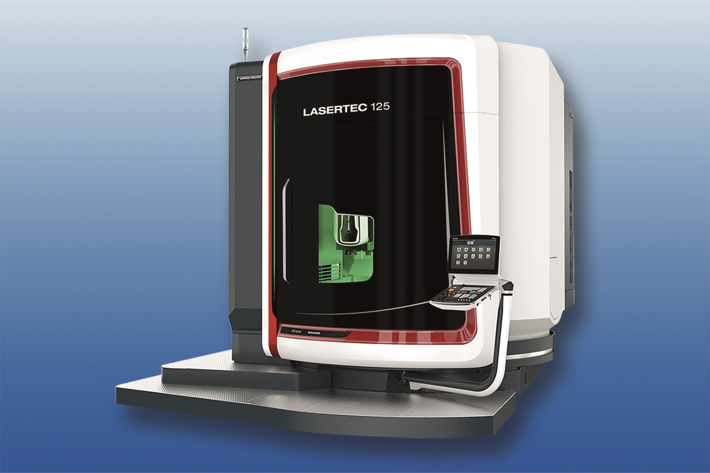
The individual components were incorporated into a machine based on the Lasertec 125 from DMG Mori. The developers had two key goals: firstly, that the machine should be easy to operate, without requiring any specialist expertise in the technologies used, and, secondly, that the number of processes should be reduced to a minimum. The simplicity of the processes represents one of the main advantages over etching, which frequently still relies on the instincts and dexterity of the machine operator.
The software plays a key role in making the fully automatic eight-axis machine easy to use. The team at RWTH Aachen University developed special tools that enable users to precisely simulate the desired structures on the surfaces and visualize their appearance in real time.
The machine’s new process control system also makes it possible to perform several tasks in succession in the same clamping. For example, the laser can be used to remove layers of black oxide left behind after laser structuring. The engineers at Fraunhofer ILT have even filed a patent application for the USP laser polishing technology developed as part of the eVerest project. A photonic process chain can be created by arranging the laser structuring, laser cleaning and laser polishing processes in sequence.
Rapid laser structuring for multiple applications
The process itself is now being tested in collaboration with partners at Volkswagen, but the potential applications of the core technology extend far beyond the confines of the auto industry. From embossing rollers in the printing industry to large bearings for rotor shafts in wind turbines, structured and functional surfaces are required across a broad variety of sectors.
“A detailed understanding of the process is essential whatever the application. The key is to combine this with modifications to the process technology and comprehensive control software,” says Andreas Brenner, summing up the project team’s approach.
Presentation of the eVerest project at LASER World of PHOTONICS in Munich
From June 24 to 27, visitors to the fair can learn more about the results of this collaborative research project at the joint Fraunhofer booth 431 in hall A2. The project will also be presented as part of an application panel on the automation of laser applications which is scheduled to be held from 3:00 p.m. to 5:20 p.m. on June 26 at the Laser Materials Processing forum in hall A3, booth 545 at LASER World of PHOTONICS.
The eVerest project was funded by the German Federal Ministry of Education and Research (BMBF) and coordinated by Project Management Agency Karlsruhe (PTKA) from January 1, 2016 through June 30, 2019. It includes the following project partners: Sauer GmbH (coordinator), Amphos GmbH, Scanlab GmbH, Precitec Optronik GmbH, Volkswagen AG, Fraunhofer ILT, the Photonics Laboratory at Münster University of Applied Sciences, and the Computer Graphics and Multimedia group at RWTH Aachen University.
Project eVerest: “Machine and systems technology for the efficient production of large-format 3D mold tools with design surfaces“
 Fraunhofer Institute for Laser Technology ILT

