Thin Film Laser Processing

Brochure Thin Film Laser Processing

Thin films are a powerful tool for improving performance and increasing the scope of technical components in many areas of modern life. The Fraunhofer Institute for Laser Technology ILT develops customized solutions for various applications.

Heat Treatment of Thin Films

In many cases thin film processing is a 2-step process involving deposition of the film followed by heat treatment. The most common deposition techniques are printing (e.g. inkjet, screen printing) for wet chemical (nanoparticle) materials and plasma processes. Typical film thicknesses are in the range of 0.1 to some microns. In order to obtain the required functionality of the film, in many cases thermal post-treatment is essential for crystallization, annealing, drying or sintering of the film material. The production of functional thin films on thermally sensitive substrates in particular represents a challenge because the thermal post-treatment process requires temperatures that exceed the temperature stability point of the substrate. Laser treatment overcomes this drawback by virtue of its rapid heating and cooling rates that allow the required temperatures to be reached in the film without affecting the substrate material. What’s more, the ability to treat layers locally and selectively opens up new possibilities in the creation of customized surface properties. Furthermore laser-based techniques are ideal for inline processing.

Wear-Protection Coatings

Wear-protection coatings are essential for improving the performance and service life of many technical devices. In the automobile sector millions of parts have to be coated every year. But there are many other fields, such as aviation and renewable energy, that widen the applications scope for wear-resistant coatings. Given the need for high throughput, optimization of the production technology for these versatile coatings is of great interest. Wet-chemical coating techniques using nanoparticulate materials hold great potential because they can be applied by using energy- and resource-saving techniques such as dip/spin coating or printing. They enable a significant reduction in production costs and energy consumption. One major challenge for these innovative coating technologies is the need for thermal post-treatment to generate the desired coating functionalities. Temperatures > 1000 °C have to be generated to achieve a significant increase in coating hardness and mechanical stability.

Thanks to the short interaction times between the laser beam and the coated component, laser-based thermal post-treatment makes it possible to attain the required high peak temperatures while minimizing the thermal load on the substrate. As a result, wear protection coatings with thicknesses between 0.1 - 1 µm and hardness in the range of 1000 HV can be produced on substrates with low tempering resistance.

Functional Films for Electronic Applications

Nanoparticulate dispersions have proven to be a powerful source for producing functional layers. Printing techniques show great potential for applying these materials because they permit resource-efficient, flexible and low-cost application of structures only onto desired areas of the substrate. This represents a considerable challenge, however, as the thermal treatment of the dried films, needed to achieve functional properties, often requires temperatures that exceed the temperature stability of the substrate (especially on polymer or glass). The laser beam offers the possibility of overcoming these drawbacks with high heating and cooling rates. In past projects Fraunhofer ILT successfully used laser treatment to functionalize inkjet-printed transparent conductive oxide coatings (TCO) based on nanoscale indium tin oxide (ITO), which is used as a transparent anode material e.g. for organic LEDs (OLED).

Post-processing with laser radiation is a key process step for obtaining layers with appropriate functionality such as high conductivity and transparency.

In various projects other functional printed layers like conductive paths, tin pads for soldering optical components and functionalities based on crystallization have been produced.

Production of Metallic Conductive Paths

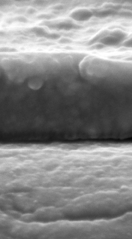
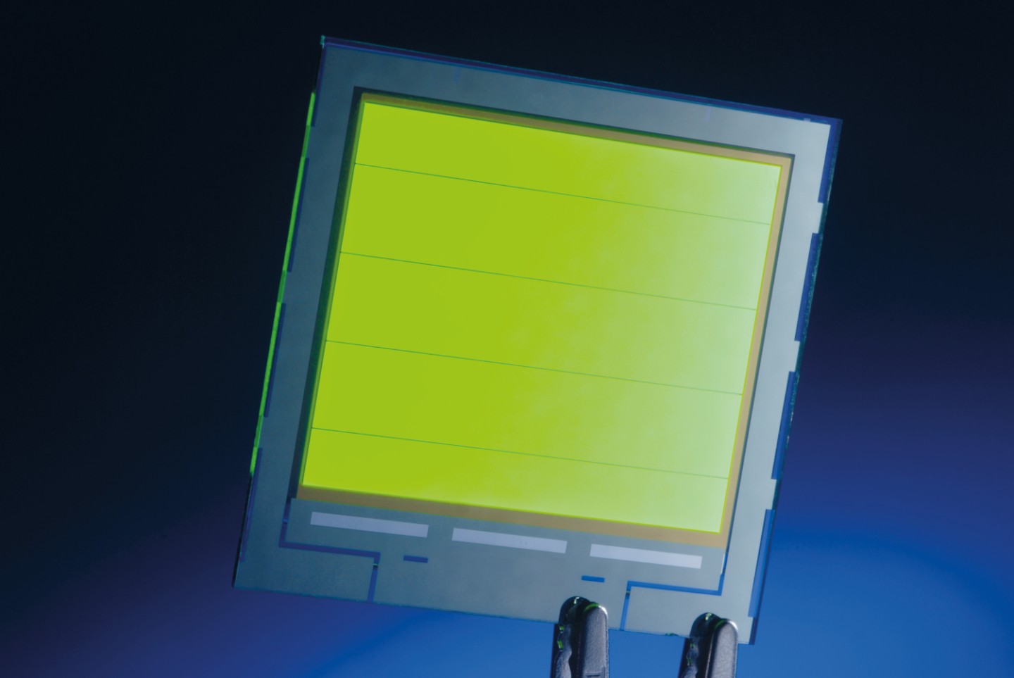
Conductive paths collect and distribute electricity on poorly or non-conducting surfaces of OLEDs, solar cells, heated windows, etc. In most cases the metallic paths can only be produced conventionally with a great deal of effort, incurring high costs for plant, equipment and energy. Electrical conductors in an OLED, for example, are produced subtractively, by photolithographic removal of aluminum previously sputtered onto the surface. More than 90% of the material applied in a cost-intensive high-vacuum sputtering process is removed using etchants. To preserve the OLED’s homogeneous luminosity, the conductive paths need to be as narrow as possible. This same requirement also applies to solar cells, although less for eye-appeal than for technical reasons - in this case the conductive paths cover the silicon surface which is important for the production of electrical energy.

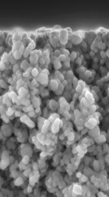
The laser-based technique which has been developed at Fraunhofer ILT produces metallic conductive paths made of aluminum, copper, silver or similar materials, in widths between 30 and 120 µm, thicknesses between 2 and 15 µm and with a maximum sheet resistance of 0.05 Ω/sq. The process takes place in ambient atmosphere at a speed of up to 2.5 m/s and can be used to manufacture conductive paths for OLEDs, heated windows, solar cells, etc.